Graduate School of Engineering
Osaka University
2-1 Yamadaoka, Suita, Osaka 565-0871 Japan
Phone and FAX number: +81-6-6879-7286
 |
Department of Precision Science and Technology Graduate School of Engineering Osaka University 2-1 Yamadaoka, Suita, Osaka 565-0871 Japan Phone and FAX number: +81-6-6879-7286 |
| |
Japanese page |
| Welcome to Yamauchi Lab. Homepage !! | Today |
|---|
| Special topic |
|---|
 |
|
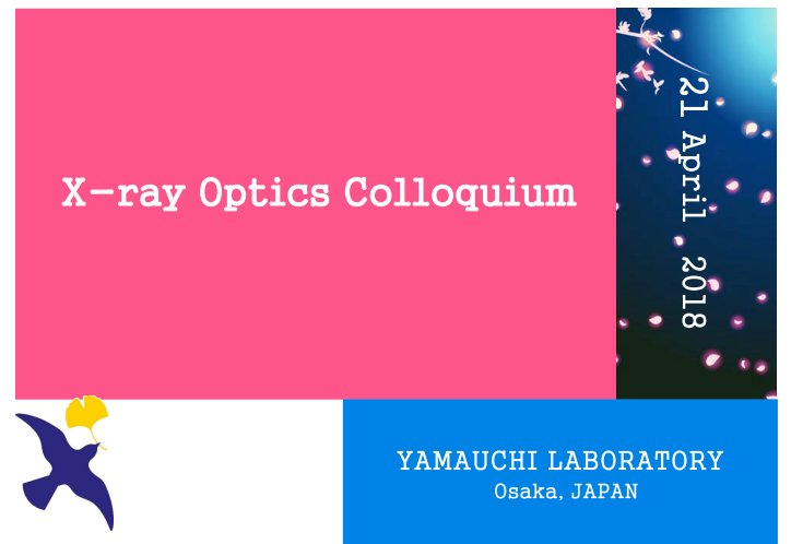
We will hold an X-ray optics colloquium on 21st (Sat) April, 2018 in Osaka as a satellite meeting of XOPT 2018 (Link-XOPT2018-).
The aim of this colloquium is to discuss about latest topics relating to X-ray optics and its application. This year, we especially foucs on adaptive X-ray optics for the next generation SR and XFEL based microscopy and on diffraction microscopy. Program Contact: Kazuto Yamauchi (yamauchi@prec.eng.osaka-u.ac.jp) |
| Introduction |
|---|
| Our laboratory researches the giant-scale nanotechnology that enables us
to fabricate atomically controlled surfaces with the size of more than
several hundreds of millimeters. In recent years, nano-fabrication and
nano-measurement methods such as EEM (elastic emission machining), PCVM
(plasma chemical vaporization machining), UPW-ECM (ultrapure water electro-chemical
machining), CARE (catalyst referred etching), MSI (microstitching interferometry),
RADSI (relative-angle determinable stitching interferometry) were successfully
developed and actually applied to fabricating atomically smoothed semiconductor
wafers, high-performance electronic and optical devices, X-ray optical
devices, SR based X-ray microscopy system, and so on. Such cutting-edge products or instruments contribute to the many scientific fields including biology, medical and pharmaceutical sciences, semiconductor device technology, and X-ray free electron laser optics etc. In educational viewpoint, students study not only their intrinsic research themes in the fields of nano-processing and nano-metrology, but also the additional themes concerning to the other groups of the different research fields, with which they are collaborating. The multi-major education is a unique system of our laboratory automatically realized in our collaborative works with the different groups. |
 |
| Webmaster |
| All Rights Reserved. Copyright (c) 2003 Osaka University |